3D machine vision opens up new perspectives for AOI (Automated Optical Inspection)
A new dimension of quality control
Miniaturisation in the field of semiconductor technology proceeds unimpeded. The development of increasingly smaller components and integrated circuits requires not only extremely precise production processes, but also new, innovative methods of quality control. The use of high-resolution 3D line scan cameras is one method.
The reliability of integrated circuits in real life parameters depends on the quality of the components, connections and contacts used. This applies especially when connection technologies like wire bonds are used, i.e. the connections of an integrated circuit or a discrete semiconductor are joined to the electrical connections of the chip housing with extremely fine wires.
The inspection of bonds is usually a combination of a mechanical, electrical and optical inspection process. There is a series of defects which cannot be detected in the course of a mechanical and electrical inspection, such as checking how high the bonds are, assuring there is sufficient space between the wire connections, recognizing any detachment at contact points (wire bond lift off) and noticing missing connections or dangerous contact points due to crossing bonds. Furthermore, the use of contact-based methods for quality control entails the risk of electrostatic and physical damage.
3D image capture
Compared to alternative systems, completely stereoscopic image capture systems of the youngest generation are of great advantage. 2D and 3D visualizations are combined in a single camera. The 3DPIXA color line scanning camera developed by Chromasens has an optical resolution of 5μm for two-dimensional color visualization and of 1μm for three-dimensional image capture. This high resolution is the basic requirement for the inspection of wire bonds with a thickness inferior to 1mil (1/1000 inch = 0,0254 Millimeter).
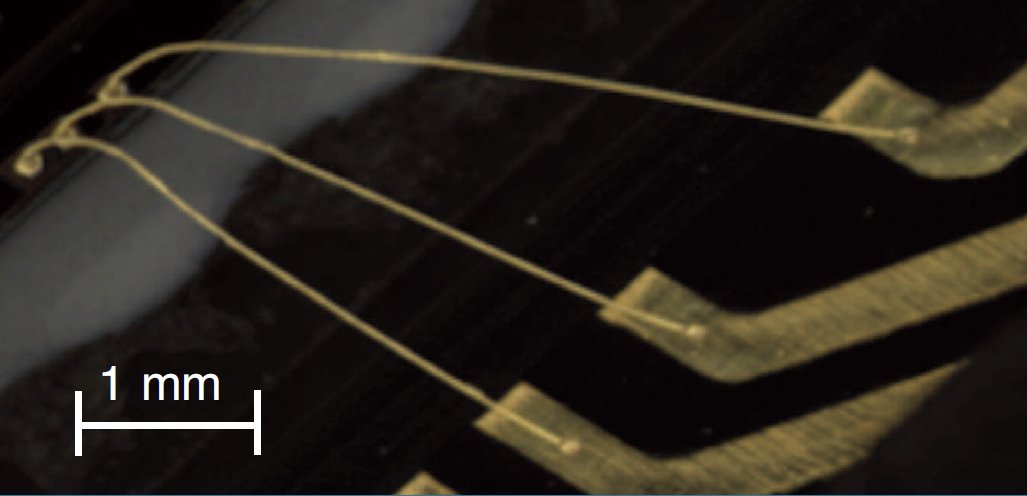
3D-Point Cloud of Wire Bond Connections
The observation of connection wires from different angles usually leads to parallax errors. The high-speed 3D algorithms developed by Chromasens clearly identify the wire connections in the generated stereo images. The data thus collected form the basis for the correlation needed to calculate the height of the wire connections. Another premise for determining the exact condition of the bonds and their geometry is optimal lighting. Lighting methods specially developed by Chromasens on the basis of homogeneous LED white light account for high-quality 3D results. Contrary to an area scan camera, the 3DPIXA as a line scan camera is capable of capturing images at an extremely rapid pace. This in turn leads to many advantages which go beyond the typical field of application where the in-line inspection of bonding connections is concerned.
PCB compatible
The automated printed circuit board inspection (AOI, Automated Optical inspection) of equipped and unequipped PCBs is an application field with enormous potential. During the inspection process, the correct assembly and connection of practically all the fitted electronic components, such as BGAs, SMDs, IC chips, resistors, capacitors and LEDs is checked. Color imaging facilitates fault detection not only by fast recognition of production errors, but also by a colored reproduction of the assembled components. 3D imaging furthermore enables the measuring of critical factors, such as the thickness of the circuit path or the integrity of bonding contacts. Defective soldering, foreign particles or possibly faulty positioning of components can also be automatically detected. Laser markings can be identified by using integrated dark field lighting.
The 3DPIXA is equally suitable for PCBs with elevations of different heights. It enables a maximum scan speed of 1360 cm2/s with an optical resolution of 30μm at a consistent height resolution of 5μm. If higher resolutions are required, such as 5μm optical resolution at a height resolution of 1μm, the scan speed is reduced to 35 cm2/s. The user can choose from camera systems with scan widths from 35 mm to 650 mm.
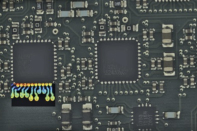
High resolution color illustration of PCBs (Printed Circuit Boards)
Amongst other factors, this high-speed inspection is due to a rapid image capture by intelligent GPUs (Graphics Processor Units) which ensure real-time processing. A flexible 3D-API (Application Programming Interface) offers users an easy control of all camera functions as well as simple integration of the AOI function in existing applications. For instance, the API can easily be linked with image processing libraries from Halcon, LabView or Matrox. Collaboration with other providers is ongoing. Application Note on the same topic can be downloaded here